Is the trigger circuit related information normal?
After the standby condition detection is normal, the trigger signal in the trigger circuit is detected whether the jump-off is normal or not. The common trigger signals are PWRBITN#, SLP_S3#, PSON#. Trigger circuit maintenance methods are as follows.
(1) First distinguish the main board trigger circuit working mode, common main board trigger circuit work as follows.
Intel, nVIDIA, AMD chipset motherboard: Switch, IO chip, south bridge chip, IO chip green wire.
VIA chipset motherboard: Switch south bridge chip transistor green wire.
SIS chipset motherboard: Switch South Bridge chip green cable.
Intel original motherboard: Switch South Bridge chip IO chip, detect CPU green cable.
IBM, DELL motherboard: Switch South Bridge chip IO chip green cable.
(2) Measuring the corresponding trigger signal.
a) Most of the motherboards are triggered by IO chips in the existing motherboard maintenance, so to measure the trigger signal you must measure the IO chip-related pins. Common IO chips trigger pin as follows.
Pin of IT8702, IT8712, IT8716, 1T8718, 1T8720, IT8721, 1T8726, 178728: 67 powered, 75 72 71 76 (GB plus 31).
IT8758 pin: 2, 31 power, 35 33 32 36.
Pin position of W83627: 61 Power, 68 67 73 72.
Pin position of F71872: 67 power, 75 72 71 76.
Pin position of F71862, 71882, 71883: 68 electricity, 80 81 82 83.
Pin position of F71889: 65 power supply, 76 77 78 79.
Note: IT8705, W83697, W83687 are not triggered.
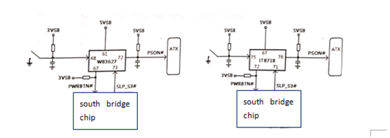
b) The trigger circuit block diagram commonly composed of Huabang and Lianyang I 0 chips is shown in figure 3.

(a) Huabang (h) Lianyang
figure 3 IO chip trigger block diagram.
Huabang and Lianyang 1O chip corresponding to normal foot jump mode: trigger switch before triggering switch triggering switch after.
W83627 Series.
The 68 pin are high level low level high level.
The 67 pin are high level low level high level.
The 73-pin is low or high-level continuous high-level.
The 72-pin is high-level sustained low-level.
ITE series (except IT8711).
The 75-pin is high-level low-level high-level.
The 72-pin is high-level low-level high-level.
The 71-pin is low or high-level continuous high-level.
The 76-pin is high-level sustained low-level.
(3) Abnormal maintenance method of trigger signal.
Using W83627 series IO chip motherboard, trigger circuit maintenance ideas are as follows. a. if the switch does not have a high level, check the pull-up resistance, capacitance, and IO chip of the switch for damage.
b. if the switch has a high level, but presses the switch 68 pin without jumping, check the line (run) from the switch to 68 pin.
c. if the 67 pin in front of the switch do not have 3.3V, check first whether the power supply to the IO chip is normal or not. If normal first change the IO chip, and finally change the South Bridge chip.