Infineon Announces Power Modules for xEV Main Inverters Creates a Cost-Effective Electric Vehicle Portfolio
Recently, Infineon Technologies AG (FSE code: IFX / OTCQX code: IFNNY) released power modules for xEV main inverters to support the automotive industry to create a wide range of high Cost-effective hybrid electric vehicle and pure electric vehicle (xEV) product portfolio. At this year's PCIM trade show, Infineon exhibited four new HybridPACKTM drive modules optimized for different inverter performance levels from 100 kW to 200 kW. In addition, the HybridPACK double-sided cooling (DSC) S2 from Infineon is an upgraded version of the existing HybridPACK DSC. This module targets the main inverters in hybrid electric vehicles and externally-charged hybrid vehicles that require high power density, with performance up to 80 kW.
HybridPACK drive - delivers flexible scalability in the same size
All new HybridPACK drive modules are designed in the same form factor as the prestigious lead product in the family of products (FS820R08A6P2x). Thanks to this, system developers can quickly and flexibly expand inverter performance without drastically changing the system design.

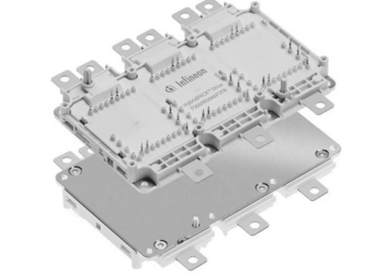
Caption: The HybridPACKTM Drive Flat module is optimized for cost-effective operation for 100 kW inverters
As a low-performance product in this family, the new HybridPACK Drive Flat modules (FS660R08A6P2Fx) and Wave modules (FS770R08A6P2x) are optimized for cost-effective applications for 100 kW to 150 kW inverters. Their substrates are connected to the inverter heatsink, but their heat dissipation performance varies depending on the substrate structure. The Flat module does not use a mature PinFin substrate that achieves the highest heat dissipation performance, but uses a flat substrate that has no structure at all. This can reduce costs but lower output power. The Wave module uses a ribbon bond wire substrate structure to compensate for the performance gap between the flat panel model and the PinFin substrate model.
This article is from Allicdata Electronics Limited.
Infineon Announces Power Modules for xEV Main Inverters Creates a Cost-Effective Electric Vehicle Portfolio
Recently, Infineon Technologies AG (FSE code: IFX / OTCQX code: IFNNY) released power modules for xEV main inverters to support the automotive industry to create a wide range of high Cost-effective hybrid electric vehicle and pure electric vehicle (xEV) product portfolio. At this year's PCIM trade show, Infineon exhibited four new HybridPACKTM drive modules optimized for different inverter performance levels from 100 kW to 200 kW. In addition, the HybridPACK double-sided cooling (DSC) S2 from Infineon is an upgraded version of the existing HybridPACK DSC. This module targets the main inverters in hybrid electric vehicles and externally-charged hybrid vehicles that require high power density, with performance up to 80 kW.
HybridPACK drive - delivers flexible scalability in the same size
All new HybridPACK drive modules are designed in the same form factor as the prestigious lead product in the family of products (FS820R08A6P2x). Thanks to this, system developers can quickly and flexibly expand inverter performance without drastically changing the system design.

Caption: The HybridPACKTM Drive Flat module is optimized for cost-effective operation for 100 kW inverters
As a low-performance product in this family, the new HybridPACK Drive Flat modules (FS660R08A6P2Fx) and Wave modules (FS770R08A6P2x) are optimized for cost-effective applications for 100 kW to 150 kW inverters. Their substrates are connected to the inverter heatsink, but their heat dissipation performance varies depending on the substrate structure. The Flat module does not use a mature PinFin substrate that achieves the highest heat dissipation performance, but uses a flat substrate that has no structure at all. This can reduce costs but lower output power. The Wave module uses a ribbon bond wire substrate structure to compensate for the performance gap between the flat panel model and the PinFin substrate model.
This article is from Allicdata Electronics Limited.
The main characteristic of the diode is Danxian
The main characteristic of the diode is Danxian.
First,the main parameters of the diode.
Maximum current.
It refers to the maximum positive current allowed to pass through the diode during long-term operation,which is related to PN junction area and external heat dissipation conditions.
Maximum reverse voltage.
When the reverse voltage at both ends of the diode reaches a certain value,the diode will be broken down and lost.
Go to unidirectional electrical conductivity.
Reverse current.
Reverse current refers to the reverse current flowing through the diode under the specified temperature and maximum reverse voltage.The smaller the reverse current,the better the one-way conductivity of the tube.
Two,the identification of the diode.
Appearance recognition.
Model identification.
Three.Detection of diode.
Use a pointer type multimeter.
RX100 and RXlk gears are usually used in ohmic gear.
Positive characteristic test.
The black pen of the multimeter (positive electrode inside the table) touches the positive pole of the diode,and the negative pole of the red watch pen (the negative electrode inside the table) touches the negative pole of the diode.If the needle is not placed in the middle of the dial,it is not the 0 value,but the resistance is the positive resistance of the diode.The smaller the forward resistance,the better.If the forward resistance is 0,it indicates the short circuit damage of the core.If the forward resistance is close to infinity,it explains the opening of the core.Both short circuit and circuit breakers can't be used.
Reverse characteristic test.
The red pen of the multimeter is the positive pole of the touch diode,and the black pen takes the negative pole of the touch diode.If the needle is at infinity or close to the infinity value, the diode is qualified.
Use the digital multimeter to test it.
The multimeter is adjusted to the detection diode,and the red pen and black pen are used to contact the two poles of the diode (red pen connection positive pole,black pen to negative pole),and the positive pressure drop of the diode can be displayed.Normal should be shown: silicon tube 0. 500~0.700V,germanium tube 0.150~0.300V.The voltage drop of Schottky diode is about 0.2V,the common silicon rectifier tube is about 0.7V, and the LED is about 1.8~2.3V.Replacement of the pen,the display shows that "1" is normal,because the reverse resistance of the diode is very large,otherwise it means that the diode has been broken.Both positive and negative measurements are 0 or 1, indicating that the diode is damaged.
How to Reduce the Power Consumption of the Relay
We all know that the relay pull-in current is larger than the hold current after the pull-in. If the relay is designed in consideration of this characteristic(that is, the operating current is reduced after the relay is pulled in), the purpose of reducing the power consumption of the relay can be achieved as long as the pull-in state can be reliably maintained.

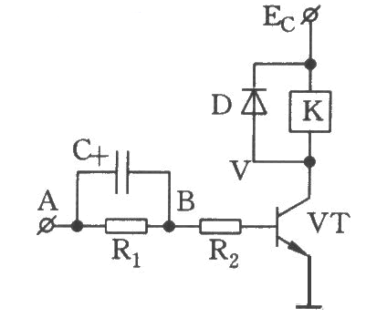
Picture 1
As shown in Picture 1, the base of the driving transistor of the relay is connected with a resistor R1 and a capacitor C. When the control level is injected from point A, the voltage across the capacitor C cannot be abruptly changed, which is equivalent to the loss of the control level of the point A injection. It is supplied to the base of the triode to drive the relay to pull in. When the voltage on the capacitor C is full, the control level is limited to R1 and then supplied to the base of the transistor, and the current of the driving relay is correspondingly reduced to maintain the pull-in, thereby achieving the purpose of reducing power consumption.

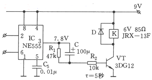
Picture 2
Let’s take a look at Picture 2. This is a circuit that provides control levels from a 555 time base circuit. When the 3 pin of the 555 circuit is flipped from a low level to a high level, since the voltage across the capacitor C cannot be abruptly changed, the injection current obtained by the triode VT is (VA-0.7V)/R2. After that, C charges through the R2 and triode eb junctions, and the VB voltage drops. When C is full, VB=VA-VC, the current Ic flowing through the relay is reduced close to releasing current due to the decrease of the base current Ib of the triode, and the relay will co mplete the low power dimension.
This article is from Allicdata Electronics Limited. Reprinted need to indicate the source.
How to identify and detect relays?
( 1 ) Discriminant type ( AC or DC ) electromagnetic relay is divided into AC and DC, which must be distinguished in use.
Because the alternating current continuously assumes the sine change, when the current passes through the zero value, the suction of the electromagnet is zero, and then the armature will be released; with the constant change of alternating current, the armature will constantly be inhaled and released, which is bound to produce violent vibration. To prevent this from happening, a copper short-circuit ring is installed at the top of the core. The function of the short circuit ring is that when the alternating flux passes through the short circuit ring, the induced current is generated, which prevents the original magnetic field from vanishing when the alternating current passes through zero, a certain amount of suction is maintained between the armature and the yoke, thus eliminating the vibration at work. In addition, the words " AC " are often marked on the coil of the AC relay. The DC electromagnetic relay has no copper ring and is marked " DC " on the DC relay. Some relays are marked with AC / DC and are used correctly according to the nominal voltage.
( 2 ) The measuring coil resistance is based on the nominal DC resistance value of the relay, and the multimeter is placed in an appropriate electrical barrier, and the resistance value of the relay coil can be directly measured. The two stylus will be connected to the two pins of the relay coil, and the multimeter indicates that they should basically meet the nominal DC resistance of the relay.
(3)The number and category of the discriminant contacts are marked with contact and pin function diagram on the relay housing, which can be directly identified. if no annotated, the relay shell can be dismantled and the relay's contact structureis carefully observed, and the relay has several pairs of contacts, the type of each pair of contacts and which reed constitute a trigger end corresponding to a set of contacts.
(4)Check the armature work situation with the hand to move the armature, see whether the armature activity is clever, there is no card phenomenon. If the armature activity is blocked, we should find out the reason to eliminate.
In addition, you can press the armature by hand, then let go to see if the armature can return to the original position under the action of spring (or reed). Note that the return spring is easier to rust and should be used as a key inspection area.
(5)When the relay produces a sucking action, the voltage at both ends of the coil is gradually reduced, and the current readings on the table will slowly decrease. When the value is reduced to a certain value, the original armature will be released, and the data is the release voltage and the release current. The release voltage of a general relay is 10%~50% of the pull in voltage. If the release voltage of the tested relay is less than the 1/10 suction voltage, the relay should not be used any longer.
( 6 ) Measurement of contact resistance
The resistance of the normally closed contact is first measured with a multimeter RX1 block, and the resistance should be zero. Then measure the resistance of the normally open contact, the resistance should be infinite. Then press the armature, when the normally open contact is closed, the resistance becomes zero; normally closed contacts turn on, and the resistance becomes infinite. If the static and dynamic contact is not changed properly, the corresponding reed can be gently moved to make it fully closed or open. The relay can no longer be used if the contact resistance is great or the contact has melted after the contact is closed. If the contact resistance is large and unstable after the contact is closed, the contact point is intact, but the surface color is black, and then the fine sand paper is applied to wipe the contact surface, make it come in good contact.
( 7 ) It is estimated that the contact load of the relay should be known exactly, and the relevant manual or information should be consulted, but sometimes it can be estimated by experience. Generally, the relay with large contact points, armature and powerful, simple and large size relays, has a relatively large contact load. Note that in several of the above measurements, DC should be used to test DC relays. If the AC relay is measured, then the AC power supply should be used, and the corresponding multimeter should also use AC 50mA blocking circuit.
If you want to know more, our website has product specifications for relays, you can go to Allicdata Electronics Limited to get more information
What are the benefits of choosing a CPLD?
1. A large number of I/O
One of the benefits of CPLD is that it provides more I/Os at a given device density, sometimes as high as 70%.
CPLD: XC2C128-7VQG100C

2. Timing model is simple
CPLD is superior to other programmable structures in that it has a simple and predictable timing model. This simple timing model is mainly due to the coarse-grained nature of the CPLD.
CPLDs can provide a wide equal state for a given time, regardless of routing. This capability is the key to successful design, not only speeding up the initial design work, but also speeding up the design and debugging process.
3. Advantages of coarse-grained CPLD structure
The CPLD is a coarse-grained structure, which means that the path to and from the device passes through fewer switches, and the corresponding delay is also small. Therefore, CPLDs can operate at higher frequencies and have better performance than equivalent FPGAs.
4. Another benefit of CPLD is that its software is compiled fast because its easy-to-route structure makes deployment design tasks easier to perform.
5. Advantages of coarse-grained CPLD structure
The FPGA is a fine-grained structure, which means there is a fine grain delay between each cell. If you align a small amount of logic together, the FPGA is quite fast. However, as the design density increases, the signal has to pass through many switches, and the routing delay increases rapidly, which diminishes overall performance. The coarse structure of the CPLD is well adapted to this design layout change.
6. Flexible output pins
The coarse-grained structure and timing characteristics of CPLDs are predictable, so designers can still change the output pins later in the design flow while the timing remains the same.
7. New CPLD package
CPLDs come in a variety of densities and package types, including single-chip self-booting solutions. The self-booting scheme integrates FLASH memory and CPLD in a single package without the need for an external boot unit, reducing design complexity and saving board space. A higher device density shares the pin output within a given package size. This gives the designer the convenience of an "zoom in" design without having to change the pinout on the board.
If you want to know more, our website has product specifications for CPLD and FPGA, you can go to ALLICDATA ELECTRONICS LIMITED to get more information
What are the benefits of choosing a CPLD?
1. A large number of I/O
One of the benefits of CPLD is that it provides more I/Os at a given device density, sometimes as high as 70%.
CPLD: XC2C128-7VQG100C

2. Timing model is simple
CPLD is superior to other programmable structures in that it has a simple and predictable timing model. This simple timing model is mainly due to the coarse-grained nature of the CPLD.
CPLDs can provide a wide equal state for a given time, regardless of routing. This capability is the key to successful design, not only speeding up the initial design work, but also speeding up the design and debugging process.
3. Advantages of coarse-grained CPLD structure
The CPLD is a coarse-grained structure, which means that the path to and from the device passes through fewer switches, and the corresponding delay is also small. Therefore, CPLDs can operate at higher frequencies and have better performance than equivalent FPGAs.
4. Another benefit of CPLD is that its software is compiled fast because its easy-to-route structure makes deployment design tasks easier to perform.
5. Advantages of coarse-grained CPLD structure
The FPGA is a fine-grained structure, which means there is a fine grain delay between each cell. If you align a small amount of logic together, the FPGA is quite fast. However, as the design density increases, the signal has to pass through many switches, and the routing delay increases rapidly, which diminishes overall performance. The coarse structure of the CPLD is well adapted to this design layout change.
6. Flexible output pins
The coarse-grained structure and timing characteristics of CPLDs are predictable, so designers can still change the output pins later in the design flow while the timing remains the same.
7. New CPLD package
CPLDs come in a variety of densities and package types, including single-chip self-booting solutions. The self-booting scheme integrates FLASH memory and CPLD in a single package without the need for an external boot unit, reducing design complexity and saving board space. A higher device density shares the pin output within a given package size. This gives the designer the convenience of an "zoom in" design without having to change the pinout on the board.
If you want to know more, our website has product specifications for CPLD and FPGA, you can go to ALLICDATA ELECTRONICS LIMITED to get more information